
MC14584B Hex Schmitt Trigger
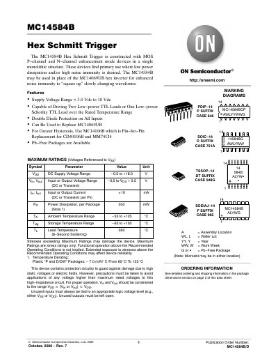
The MC14584B/DMC14584B Hex Schmitt Trigger is a MOS P‑channel and N‑channel enhancement mode device intended for low‑power, high‑noise‑immunity applications. It can replace the MC14069UB hex inverter to improve noise immunity and "square up" slowly changing waveforms.
Key specifications include a supply voltage range of 3.0 V to 18 V, the ability to drive two low‑power TTL loads (or one Schottky TTL load), double diode protection on all inputs, and a maximum input/output current of ±10 mA per pin. The device is offered in PDIP‑14, SOIC‑14, TSSOP‑14, and SOEIAJ‑14 packages, with Pb‑free options available.
| Supply Voltage Range | 3.0 Vdc to 18 Vdc |
|---|---|
| Input/Output Current per Pin | ±10 mA |
| Ambient Temperature Range | -55 °C to +125 °C |
| Storage Temperature Range | -65 °C to +150 °C |
| TTL Load Capability | Two low‑power TTL loads or one low‑power Schottky TTL load |
The device operates from 3.0 Vdc up to 18 Vdc.
It can drive two low‑power TTL loads, or one low‑power Schottky TTL load.
Each pin can handle up to ±10 mA of current.