
The MC14551B is a digitally-controlled analog switch. This device implements a 4PDT solid state switch with low ON impedance and very low OFF Leakage current. Control of analog signals up to the complete supply voltage range can be achieved.
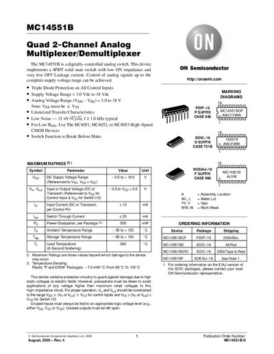
The MC14551B from ON Semiconductor is a digitally‑controlled analog switch that implements a 4‑pole‑double‑throw (4PDT) solid‑state configuration. It supports supply voltages from 3 V to 18 V and analog signal ranges up to the same limits, with triple diode protection on all control inputs.
The datasheet provides detailed electrical characteristics, maximum ratings, pin assignments, test circuit diagrams, application examples, and mechanical package dimensions for both PDIP‑16 and SOIC‑16 versions.
| Supply Voltage Range | 3.0 V DC to 18 V DC |
|---|---|
| Analog Voltage Range (Vpp‑Veg) | 3.0 V to 18 V |
| Maximum Power Dissipation (per package) | 500 mW |
| Ambient Temperature Range | -55 °C to +125 °C |
| Storage Temperature Range | -65 °C to +150 °C |
| Control Input Propagation Delay (typical) | 20 ns |
The device operates from 3.0 V DC up to 18 V DC.
The maximum power dissipation is 500 mW per package.
It is a quad device, offering four 2‑channel analog multiplexers/demultiplexers.
Unused inputs must be tied to an appropriate logic voltage level such as Vgg, Vee, or Vpp.