
This is a logic IC datasheet, which introduces the features and characteristics of HC112 and HCT112, including operating voltage range, input and output voltage range, output load capacity, operating temperature range, propagation delay and transition time.
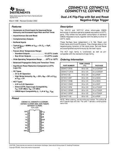
The CD74HC112 and CD74HCT112 are dual J‑K flip‑flops with independent set and reset inputs. They feature hysteresis on clock inputs, buffered inputs, complementary outputs, and operate on the negative‑edge of the clock. The HC version works from 2 V to 6 V, while the HCT version is compatible with LSTTL logic and operates from 4.5 V to 5.5 V.
The document provides detailed pinout diagrams, functional diagrams, truth tables, absolute maximum ratings, electrical and switching specifications, as well as packaging and ordering information for multiple package types such as PDIP, SOIC, SOP, TSSOP and CERDIP.
| Typical maximum frequency (f_MAX) | 60 MHz at VCC = 5 V, CL = 15 pF |
|---|---|
| Supply voltage range (HC types) | 2 V to 6 V |
| Operating temperature range | -55 °C to 125 °C |
| Quiescent device current (HC types) | 6 µA |
The device can operate up to 60 MHz when powered at 5 V with a 15 pF load capacitance.
Both devices are rated for operation from –55 °C to 125 °C.