
This document is about the packaging information of products JM38510/30109B2A, JM38510/30109BEA, JM38510/30109BFA, JM38510/30109SEA, JM38510/30109SFA, SN54LS109AJ, SN74109N, SN74LS109AD, SN74LS109ADE4, SN74LS109ADG4, SN74LS109ADR
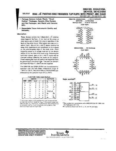
The SN54109, SN54LS109A, SN74109 and SN74LS109A are dual J‑K positive‑edge‑triggered flip‑flops with independent preset and clear inputs. A low level on preset or clear forces the corresponding output high or low regardless of other inputs. When both are inactive, data on the J and K inputs are transferred to the outputs on the rising clock edge.
The devices are offered in several package styles (plastic “Smail”, ceramic chip carriers, flat packages, DIP, SOIC, CFP) and are characterized for operation over a wide temperature range. Electrical specifications include a 4.5 V–5.5 V supply range, 2 V high‑level input, 0.8 V low‑level input, up to 33 MHz clock frequency, and output currents up to 16 mA.
| High‑level output current | -0.8 mA |
|---|---|
| Maximum clock frequency | 33 MHz |
| Operating temperature range (SN54109) | -55 °C to 125 °C |
It is specified for a military temperature range of –55 °C to 125 °C.
The devices support clock frequencies up to 33 MHz.