
SN54HCT32, SN74HCT32 are four independent 2-input OR gates. They operate in a positive logic. Their operating voltage range is 4.5V to 5.5V. The output current can drive 10 LSTTL loads. The power consumption is low, with a typical propagation delay of 13ns, an output current of ±4mA at 5V, and an input current of up to 1µA. The input voltage is TTL-voltage compatible.
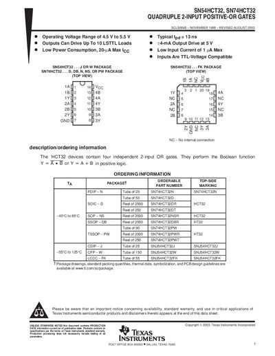
The SN54HCT32 and SN74HCT32 are quad 2‑input positive‑OR logic devices that are TTL‑compatible and operate over a 4.5 V to 5.5 V supply range. They feature low power consumption, can drive up to 10 LSTTL loads, and have typical propagation delays of about 13 ns.
The document lists detailed electrical parameters, absolute‑maximum ratings, and mechanical data for multiple package options (PDIP, SOIC, SSOP, TSSOP). It also includes ordering information, tape‑and‑reel dimensions, and an important notice about warranty and usage restrictions.
| Supply voltage range | 4.5 V to 5.5 V |
|---|---|
| High‑level input voltage (VIH) | 2 V |
| Low‑level input voltage (VIL) | 0.8 V |
| Output drive current | ±4 mA at 5 V |
| Typical propagation delay | 13 ns |
| Maximum output load | 10 LSTTL loads |
| Quiescent current (ICC) | 20 µA max |
| Available packages | PDIP, SOIC, SSOP, TSSOP |
The devices operate from 4.5 V to 5.5 V.
Typical propagation delay is about 13 ns.
Package options include PDIP, SOIC, SSOP and TSSOP.
They can source or sink up to ±4 mA at a 5 V supply.