
This document provides preliminary information on a new product that is currently in development or undergoing evaluation. The product is a programmable peripheral device that allows for data changes. It features a single supply voltage, primary flash memory, secondary flash memory, SRAM, PLD, I/O ports, and more.
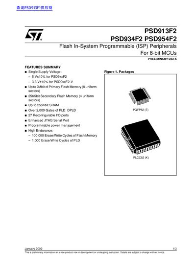
The PSD9XX family provides a configurable memory system on a chip for 8‑bit microcontrollers. Each device integrates primary flash memory, secondary flash, SRAM, programmable logic (PLD) and reconfigurable I/O ports, enabling flexible embedded designs.
Key features include up to 2 Mbit of primary flash, a 256 Kbit secondary flash, up to 256 Kbit SRAM, over 2,000 PLD gates, 27 configurable I/O pins, and an on‑chip power‑management unit with automatic power‑down. Programming can be performed in‑system via a JTAG‑compliant ISP interface or in‑application using the dual‑flash architecture.
| Supply Voltage (3.3 V version) | 3.3 V ±10% |
|---|---|
| Primary Flash Memory | Up to 2 Mbit (8 uniform sectors) |
| Secondary Flash Memory | 256 Kbit (4 uniform sectors) |
| SRAM | Up to 256 Kbit |
| Programmable Logic Gates | Over 2,000 gates (DPLD PQFP852) |
| Flash Endurance | 100,000 erase/write cycles (minimum) |
| PLD Endurance | 1,000 erase/write cycles (minimum) |
| Data Retention | 15 years |
Each device can contain up to 2 Mbit of primary flash memory.
The flash memory is rated for a minimum of 100,000 erase/write cycles.