
HCF4001B is a monolithic integrated circuit fabricated in Metal Oxide Semiconductor technology available in DIP and SOP packages. It is a quad 2-input NOR gate that provides the system designer with direct implementation of the NOR function and supplement the existing family of CMOS gates. All inputs and outputs are buffered.
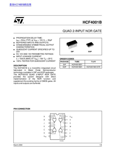
The HCF4001B is a monolithic quad 2‑input NOR gate fabricated in MOS technology and offered in DIP‑14, SOP‑14 and SO‑14 packages. All inputs and outputs are buffered, providing standardized symmetrical output characteristics for system designers.
The document lists key electrical parameters such as propagation delay, quiescent current, supply voltage range, and power dissipation, as well as mechanical dimensions for each package. Recommended operating conditions and absolute maximum ratings are also included to guide reliable circuit design.
| Propagation delay time (typ) | 50 ns at Vpp = 10 V |
|---|---|
| Supply voltage range | 3 V to 20 V |
| Power dissipation per package | 200 mW |
| Input leakage current (max) | 100 nA at Vpp = 18 V |
| Operating temperature range | -55 °C to +125 °C |
The typical propagation delay time is 50 ns when Vpp is 10 V.
The device is recommended to operate with a supply voltage between 3 V and 20 V.
Each package can dissipate up to 200 mW of power.
The maximum input leakage current is 100 nA at a Vpp of 18 V.