
The MAX2240 single-supply, low-voltage power amplifier (PA) IC is designed specifically for applications in the 2.4GHz to 2.5GHz frequency band. The PA is compliant with Bluetooth, HomeRF, and 802.11 standards, as well as other FSK modulation systems. The PA provides a nominal +20dBm (100mW) output power in the highest power mode. The PA includes a digital power control circuit to greatly simplify control of the output power. Four digitally controlled output power levels are provided: from +3dBm to +20dBm. A digital input controls the active or shutdown operating modes of the PA. In the shutdown mode, the current reduces to 0.5µA. The IC integrates the RF input and interstage matching to simplify application of the IC. Temperature and supply-independent biasing are also included to provide stable performance under all operating conditions. The IC operates from a +2.7V to +5V single-supply voltage. No negative bias voltage is required. Current consumption is a modest 105mA at the highest power level. The part is packaged in the UCSP™ package significantly reducing the required PC board area. The chip occupies only a 1.56mm x 1.56mm area. The 3 x 3 array of solder bumps are spaced with a 0.5mm bump pitch.
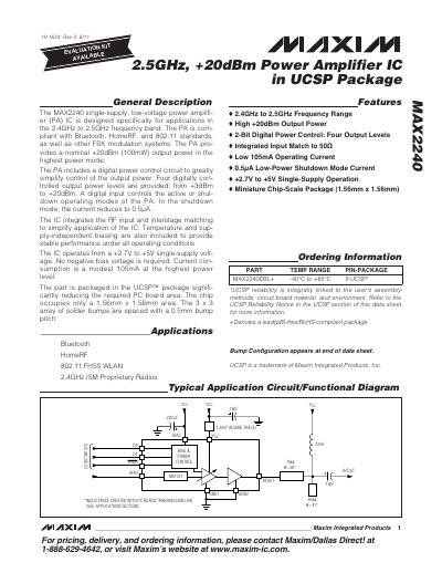
The MAX2240 is a single‑supply, low‑voltage power amplifier IC designed for the 2.4 GHz to 2.5 GHz band and compliant with Bluetooth, HomeRF, and 802.11 standards. It delivers up to +20 dBm (100 mW) output power and features a 2‑bit digital control that provides four selectable output‑power levels.
The device operates from a +2.7 V to +5 V supply, consumes 105 mA at full power, and shuts down to a 0.5 µA standby current. It is offered in a miniature UCSP chip‑scale package (1.56 mm × 1.56 mm) with a 0.5 mm bump pitch, and includes integrated RF input matching and bias circuitry.
| Frequency Range | 2.4 GHz to 2.5 GHz |
|---|---|
| Nominal Output Power | +20 dBm (100 mW) |
| Supply Voltage | +2.7 V to +5 V |
| Maximum Supply Current | 105 mA |
| Shutdown Current | 0.5 µA |
| Package Size | 1.56 mm × 1.56 mm |
The MAX2240 provides a nominal +20 dBm (100 mW) output power in the highest power mode.
It operates from a single‑supply voltage of +2.7 V to +5 V.
Four digitally controlled output power levels are provided, ranging from +3 dBm to +20 dBm.
In shutdown mode the current is reduced to 0.5 µA.