
The MAX2630/MAX2631/MAX2632/MAX2633 are low-voltage, low-noise amplifiers for use from VHF to microwave frequencies. Operating from a single +2.7V to +5.5V supply, these devices have a flat gain response to 900MHz. Their low noise figure and low supply current make them ideal for receive, buffer, and transmit IF applications. The MAX2630/MAX2631 are biased internally, eliminating the need for external bias resistors or inductors. The MAX2632/MAX2633 have a user-selectable supply current, which can be adjusted by adding a single external resistor. This allows customized output power and gain according to specific applications requirements. The MAX2631/MAX2633 feature a shutdown pin that allows them to be powered down to less than 1µA supply current. Aside from a single bias resistor required for the MAX2632/MAX2633, the only external components needed for this family of amplifiers are input and output blocking capacitors and a VCC bypass capacitor. The MAX2630 comes in a 4-pin SOT143 package, requiring minimal board space. The MAX2631/MAX2632 come in small 5-pin SOT23 packages. The MAX2633 comes in a 6-pin SOT23 package.
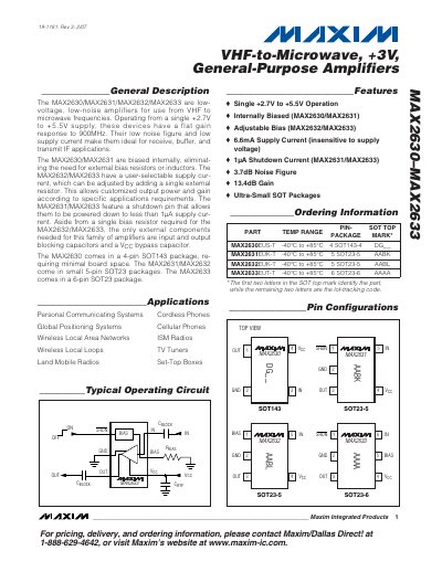
The MAX2630‑MAX2633 family are low‑voltage, low‑noise broadband amplifiers designed for VHF‑to‑microwave frequencies. They operate from a single +2.7 V to +5.5 V supply and provide a flat gain response up to 900 MHz, making them suitable for receive, buffer and transmit IF applications.
The series includes internally biased devices (MAX2630, MAX2631) and versions with user‑selectable bias current (MAX2632, MAX2633). MAX2631 and MAX2633 also feature a shutdown pin that reduces supply current to less than 1 µA. Available in ultra‑small SOT packages, the devices require only input/output blocking capacitors and a VCC bypass capacitor.
| Supply Voltage | +2.7 V to +5.5 V |
|---|---|
| Gain | 13.4 dB |
| Noise Figure | 3.8 dB |
| Typical Supply Current | 6.6 mA |
| Operating Temperature Range | -40 °C to +85 °C |
| Package (MAX2630) | 4‑pin SOT‑143 |
| Package (MAX2631/MAX2632) | 5‑pin SOT‑23 |
| Package (MAX2633) | 6‑pin SOT‑23 |
| VSWR (Output) | 1.25:1 |
The amplifiers operate from a single +2.7 V to +5.5 V supply.
The MAX2630 is offered in a 4‑pin SOT‑143 package.
The typical gain is 13.4 dB.