
The MC14049UB hex inverter/buffer is constructed with MOS P–channel and N–channel enhancement mode devices in a single monolithic structure. This complementary MOS device finds primary use where low power dissipation and/or high noise immunity is desired. This device provides logic–level conversion using only one supply voltage, VDD. The input–signal high level (VIH) can exceed the VDD supply voltage for logic–level conversions. Two TTL/DTL Loads can be driven when the device is used as CMOS–to–TTL/DTL converters (VDD = 5.0 V, VOL ≤ 0.4 V, IOL ≥ 3.2 mA). Note that pins 13 and 16 are not connected internally on this device; consequently connections to these terminals will not affect circuit operation.
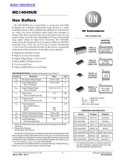
The MC14049UB is a hex inverter/buffer built with complementary MOS P‑channel and N‑channel devices in a single monolithic package. It offers low power dissipation, high noise immunity, and can operate with a single supply voltage (Vpp) while allowing input levels to exceed the supply voltage.
The document provides pin assignments, electrical and switching characteristics, package dimensions for PDIP‑16, SOIC‑16, TSSOP‑16 and EIAJ‑16, and ordering information. It also includes maximum ratings, typical performance curves, and safety notices.
| Supply Voltage Range | 3.0 V to 18 V |
|---|---|
| Input Voltage Range | -0.5 V to +18.0 V |
| Power Dissipation | Typical value in mW (see table) |
The device operates from 3.0 V up to 18 V supply voltage.
The input voltage can range from –0.5 V to +18.0 V.