
MC14099B is an 8-bit addressable latch with serial data input and parallel output functions. It can enter data in serial form when the appropriate latch is addressed (via address pins A0, A1, A2) and write disable is in the low state. The data is presented in parallel at the output of the eight latches independently of the state of Write Disable, Write/Read or Chip Enable. A Master Reset capability is available on both parts.
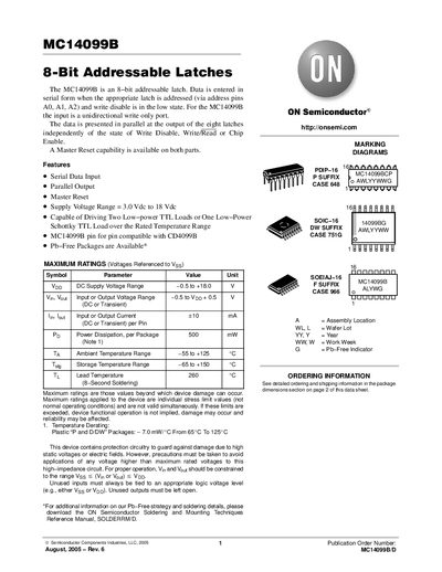
The MC14099B is an 8‑bit addressable latch from ON Semiconductor. Data is entered serially via address pins (A0, A1, A2) when write‑disable is low, and the eight latch outputs are presented in parallel regardless of control signals. The device includes a master reset and is pin‑compatible with the CD4099B.
The datasheet provides detailed electrical characteristics, maximum ratings, switching timings, and package dimensions for PDIP‑16 and SOIC‑16 variants. Ordering information lists both standard and Pb‑free package options, and the document includes pin assignments, functional diagrams, and truth tables for design reference.
| Supply Voltage Range | 3.0 V to 18 V |
|---|---|
| Input/Output Voltage Range | -0.5 V to Vpp + 0.5 V |
| Input/Output Current per Pin | 10 mA (DC or transient) |
| Power Dissipation (per package) | 500 mW |
| Ambient Temperature Range | -55 °C to +125 °C |
| Storage Temperature Range | -65 °C to +150 °C |
| Lead Temperature (soldering) | 260 °C (8‑second soldering) |
The device operates from 3.0 V up to 18 V.
Each pin can source or sink up to 10 mA (DC or transient).
The device is rated for an ambient temperature range of –55 °C to +125 °C.