
L6730 and L6730B are adjustable step-down controllers with synchronous rectification. They have an input voltage range from 1.8V to 14V and a supply voltage range from 4.5V to 14V. The adjustable output voltage can go down to 0.6V with ±0.8% accuracy over line voltage and temperature (0°C~125°C). They feature fixed frequency voltage mode control, tON lower than 100ns, and 0% to 100% duty cycle. They offer selectable 0.6V or 1.2V internal voltage reference or external input voltage reference. They have soft-start and inhibit functions, high current embedded drivers, and predictive anti-crossconduction control. They also have selectable uvlo threshold (5V or 12V BUS), programmable high-side and low-side RDS(on) sense over-current-protection, switching frequency programmable from 100kHz to 1MHz, and master/slave synchronization with 180° phase shift. The L6730 has pre-bias start up capability and selectable source/sink or source only capability after soft-start. The L6730B has selectable constant current or hiccup mode overcurrent protection after soft-start. They both have power good output with programmable delay, over voltage protection with selectable latched/not-latched mode, and thermal shut-down. They are suitable for high performance / high density DC-DC modules, low voltage distributed DC-DC, niPOL converters, DDR memory supply, and DDR memory bus termination supply.
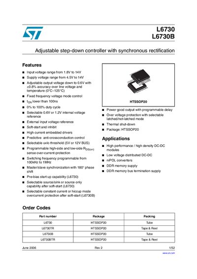
The L6730/L6730B is an adjustable step‑down controller with synchronous rectification, supporting an input voltage range of 1.8 V to 14 V and a supply voltage range of 4.5 V to 14 V. It offers an output voltage adjustable down to 0.6 V with ±0.8 % accuracy, a duty cycle of 0 %–100 %, and a minimum on‑time lower than 100 ns. The device includes programmable switching frequency (400 kHz–1 MHz), high‑current drivers, and various protection features such as over‑voltage, over‑current, and thermal shutdown.
The document contains a summary description, functional description, electrical data (maximum ratings, thermal data), pin connections and functions, electrical characteristics, and application notes such as inductor design and compensation network. Pin‑level details explain the multifunction pin behavior, PGOOD delay configuration, and synchronization options. Revision history and legal notices are provided at the end.