
This document is about the characteristics of TL062, which includes low power, high input impedance, high switching speed, low input bias current, low input bias voltage, temperature compensation, short circuit protection, etc.
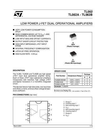
The TLO62 family comprises low‑power dual J‑FET input operational amplifiers with high slew rate, low input bias and offset currents, and internal frequency compensation. They are offered in eight‑pin plastic DIP and eight‑pin plastic micro‑package (SO) formats and support a wide common‑mode voltage range.
The document provides absolute maximum ratings, detailed electrical characteristics, mechanical dimensions, typical application circuits, and a schematic diagram. It also lists order codes for various temperature‑range versions and includes graphs of performance versus supply voltage, temperature, and load conditions.
| Supply voltage (absolute max) | +18 V |
|---|---|
| Slew rate | 3.5 V/µs |
The typical slew rate is 3.5 V/µs.
The absolute maximum supply voltage is +18 V.