
HCF4050B is a monolithic integrated circuit fabricated in Metal Oxide Semiconductor technology available in DIP and SOP packages. It is an non inverting Hex Buffer/Converter and feature logic level conversions using only one supply voltage (VDD). The input high level signal (VIH) can exceed the VDD supply voltage when these devices are used for logic level conversions. This device is intended for use as CMOS to DTL/TTL converters and can drive directly two DTL/TTL loads (VDD=5V, VOL≤0.4V and IOL≤3.2mA.
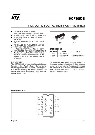
The HCF4050B is a monolithic integrated circuit fabricated in MOS technology, available in DIP‑16 and SOP packages. It functions as a non‑inverting hex buffer/level‑shifter that uses a single supply voltage (VDD) for logic level conversion, suitable for CMOS‑to‑DTL/TTL applications.
The document lists absolute maximum ratings, recommended operating conditions, DC specifications such as supply voltage range (3 V‑20 V), input leakage (100 nA), quiescent current, high/low output voltage levels, and dynamic characteristics like propagation delay and transition times. Mechanical data for the DIP‑16 and SO‑16 packages are also provided.
| Supply Voltage (VDD) Range | 3 V to 20 V |
|---|---|
| Input Leakage Current | 100 nA (max) at VDD=18 V |
| Quiescent Current (IL) | 0.02 µA at 5 V, 0.04 µA at 20 V |
| High‑Level Output Voltage (VOL) at VDD=5 V | ≥4.95 V |
| Low‑Level Output Voltage (VOL) at VDD=5 V | ≤0.05 V |
| Propagation Delay (tPD) Typical | 40 ns at VDD=10 V |
The device operates with a supply voltage from 3 V up to 20 V.
Typical propagation delay is 40 ns when VDD is 10 V.
The maximum input leakage current is 100 nA at a VDD of 18 V.