
This document describes the features and characteristics of the FQP85N06 60V N-Channel MOSFET released in May 2001. These power field effect transistors are produced using Fairchild's proprietary DMOS technology, which minimizes on-state resistance, provides superior switching performance, and withstands high energy pulse in the avalanche and commutation mode. They are suitable for low voltage applications such as automotive, DC/DC converters, and high efficiency switching for power management in portable and battery operated products.
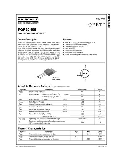
This datasheet provides the electrical, thermal, and mechanical specifications for the Fairchild FQP85N06 60 V N‑Channel MOSFET. It includes absolute maximum ratings, typical characteristics, and test circuit diagrams for evaluating performance.
Key features include a low RDS(on) of 0.010 Ω at VGS = 10 V, 85 A continuous drain current, 300 A pulsed capability, and a maximum junction temperature of 175 °C. Package dimensions and thermal resistance values are also listed for design integration.
| Drain‑Source Voltage (VDS) | 60 V |
|---|---|
| Gate‑Source Voltage (VGS) | ±25 V |
| Total Gate Charge (Qg) | 86 nC (typical) |
| Reverse Transfer Capacitance (Crss) | 165 pF (typical) |
| Maximum Junction Temperature (TJ) | 175 °C |
| Thermal Resistance Junction‑to‑Case (RθJC) | 0.94 °C/W |
| Power Dissipation (PD) at 25 °C | 160 W |
The MOSFET is rated for a gate‑source voltage of ±25 V.
The typical total gate charge is 86 nC.