
The NB6N11S is a 3.3 V 1:2 AnyLevel input to LVDS Fanout Buffer / Translator from ON Semiconductor. It can accept LVPECL, CML, LVCMOS, LVTTL or LVDS AnyLevel input signals and translate them to LVDS output signals. Two identical copies of Clock or Data will be distributed with a maximum working frequency of 2.0 GHz or 2.5 Gb/s respectively. The NB6N11S is ideal for SONET, GigE, Fiber Channel, Backplane and other Clock or Data distribution applications.
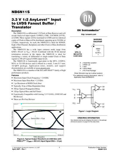
The NB6N11S receives AnyLevel input signals (LVPECL, CML, LVCMOS, LVTTL, LVDS) and translates them to LVDS, providing two identical outputs. It operates up to 2.0 GHz clock frequency or 2.5 Gb/s data rate, making it suitable for SONET, GigE, Fiber Channel and other high‑speed applications.
The device is offered in a 3 mm × 3 mm 16‑pin QFN package, features a wide input common‑mode range, internal 50 Ω termination, and includes detailed pin‑out, electrical characteristics, and ordering information.
| Maximum Input Clock Frequency | > 2.0 GHz |
|---|---|
| Maximum Input Data Rate | > 2.5 Gb/s |
| Typical Propagation Delay | 380 ps |
| Typical Rise and Fall Times | 120 ps |
| Power Supply Current | 35‑50 mA |
| Input Common‑Mode Range | GND +50 mV to Vcc − 50 mV |
| LVDS Output Voltage | 250‑450 mV |
The device accepts input common‑mode voltages from GND + 50 mV up to VCC − 50 mV.
The NB6N11S can handle data rates greater than 2.5 Gb/s.
Typical propagation delay is 380 ps.