
The NCP5662/NCV5662 is a high-performance, low dropout linear regulator designed for high power applications that require up to 2.0 A current. It is offered in both fixed and adjustable output versions. With output voltages as low as 0.9 V and ultra-fast response times for load transients, the NCP5662/NCV5662 also provides additional features such as Enable and Error Flag (for the fixed output version), increasing the utility of these devices. A thermally robust, 5 pin D2PAK or DFN8 package, combined with an architecture that offers low ground current (independent of load), provides for a superior high-current LDO solution.
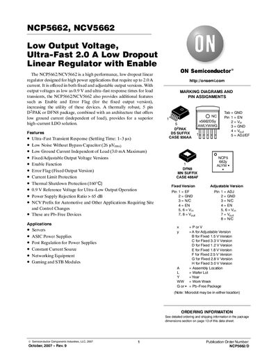
The NCP5662 and NCV5662 are ultra‑fast, 2 A low‑dropout linear regulators offered in fixed and adjustable output versions. They feature enable control, error‑flag output, low ground current and high PSRR, making them suitable for high‑power applications such as servers, ASIC power supplies and automotive electronics.
The document provides detailed electrical characteristics, absolute maximum ratings, thermal data, pin functions, typical application schematics and package dimensions for both the DPAK and DFN8 packages. Ordering information and contact details for ON Semiconductor technical support are also included.
| Maximum Input Voltage | 18 V |
|---|---|
| Maximum Junction Temperature | 150 °C |
| Thermal Resistance, Junction‑to‑Ambient (DPAK) | 45 °C/W |
| Thermal Resistance, Junction‑to‑Case (DPAK) | 5.0 °C/W |
| Dropout Voltage at 2 A | 1.0‑1.3 V |
| Output Noise Voltage (Fixed 0.9 V version) | ≤ 26 µV rms |
| Power Supply Rejection Ratio | > 65 dB |
| Low Ground Current (max) | 3.0 mA |
| Error Flag Current | 3.0 mA |
| Operating Input Voltage Range | 2 V to 9 V |
The device can tolerate up to 18 V on the input pin.
The dropout voltage is between 1.0 V and 1.3 V when delivering 2 A.
The junction‑to‑case thermal resistance is 5.0 °C/W.