
The DS90C3202 is a 3.3V single/dual FPD-Link 10-bit color receiver designed for use in Liquid Crystal Display TVs, LCD Monitors, Digital TVs, and Plasma Display Panel TVs. It interfaces between the digital video processor and the display device using the low-power, low-EMI LVDS (Low Voltage Differential Signaling) interface. The DS90C3202 converts up to ten LVDS data streams back into 70 bits of parallel LVCMOS/LVTTL data. The receiver can be programmed with rising edge or falling edge clock. Optional two-wire serial programming allows fine tuning in development and production environments. With an input clock at 135 MHz, the maximum transmission rate of each LVDS line is 945 Mbps, for an aggregate throughput rate of 9.45 Gbps (945 Mbytes/s). This allows the dual 10-bit LVDS Receiver to support resolutions up to HDTV.
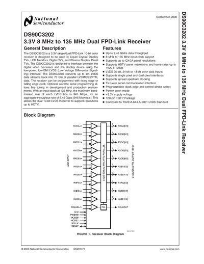
The DS90C3202 is a 3.3 V single/dual FPD‑Link 10‑bit color receiver designed for LCD TVs, monitors, digital TVs and plasma panels. It converts up to ten LVDS data streams back into 70 bits of parallel LYCMOS/LVTTL data and can be programmed for rising‑edge or falling‑edge clock operation.
Key features include up to 9.45 Gbps aggregate throughput, support for QXGA and HDTV resolutions, two‑wire serial programming, selectable output data strobe, spread‑spectrum clocking, power‑down mode, and a 128‑pin TQFP package. Electrical specifications such as supply voltage, input clock range, and pin‑out details are provided in the datasheet.
| Supply Voltage | 3.3 V |
|---|---|
| Input Clock Range | 8 MHz to 135 MHz |
| Maximum Data Throughput | 9.45 Gbps (945 Mbytes/s) |
| Supported Resolutions | Up to HDTV 1920 × 1080p, QXGA |
| Package | 128‑pin TQFP |
| LVDS Data Input Width | 30‑bit, 24‑bit or 18‑bit |
| Two‑Wire Serial Interface Speed | 400 kHz clock |
| Power‑Down Mode | Supported |
The device can handle up to 9.45 Gbps (945 Mbytes/s) of aggregate data throughput.
It operates from a 3.3 V supply.
The RFB pin selects rising‑edge or falling‑edge clock for the output data strobe.
A two‑wire serial communication interface is provided for programming and fine‑tuning.