
DS90CR483A / DS90CR484A is a 48-bit LVDS channel link SER/DES chip that supports a working frequency of 33-112MHz. It can convert 48 bits of CMOS/TTL data into 8 LVDS data streams and transmit a phase-locked transmit clock over the ninth LVDS link. The use of this chipset can significantly reduce the number of cables, reduce system costs, and reduce the physical size and cost of connectors.
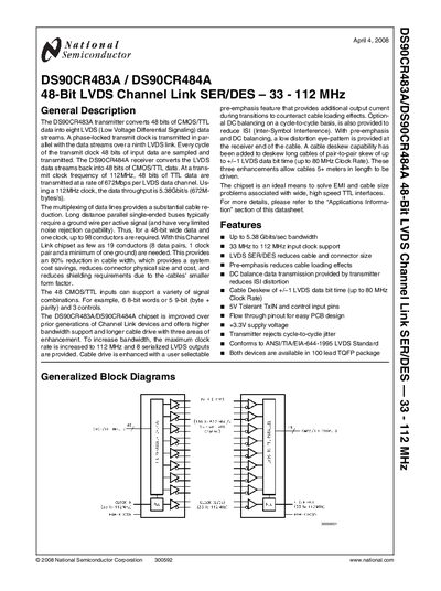
The DS90CR483A transmitter converts 48 bits of CMOS/TTL data into eight LVDS streams and adds a ninth LVDS link for the transmit clock. The DS90CR484A receiver converts those LVDS streams back to 48‑bit CMOS/TTL data, supporting clock rates from 33 MHz to 112 MHz.
Key features include up to 5.38 Gbits/sec bandwidth, pre‑emphasis and DC‑balance to reduce ISI and cable loading, cable deskew of ±1 LVDS bit time, and a reduction of required conductors from up to 98 to as few as 19. The devices are offered in a 100‑lead TQFP package.
| Maximum bandwidth | 5.38 Gbits/sec |
|---|---|
| Supported input clock range | 33 MHz to 112 MHz |
| LVDS driver differential output voltage | 250 mV to 450 mV |
| Transmitter supply current (112 MHz) | up to 210 mA |
The devices can transmit up to 5.38 Gbits per second (672 Mbytes/s) at a 112 MHz clock.
Both parts support input clocks from 33 MHz up to 112 MHz.
A pre‑emphasis feature and DC‑balance transmission reduce cable loading and ISI distortion.
The chipset reduces the required conductors from up to 98 to as few as 19 (8 data pairs, 1 clock pair, and 1 ground).