
The LM5110 is a dual 5A compound gate driver with negative output voltage capability. It can independently drive two N-channel MOSFETs and uses a composite CMOS and bipolar transistor array for output driving. The current drive capacity can reach 5A peak and can drive low threshold MOSFETs. It also has undervoltage lockout protection and a shutdown input pin. The device uses SOIC-8 and LLP-10 packages.
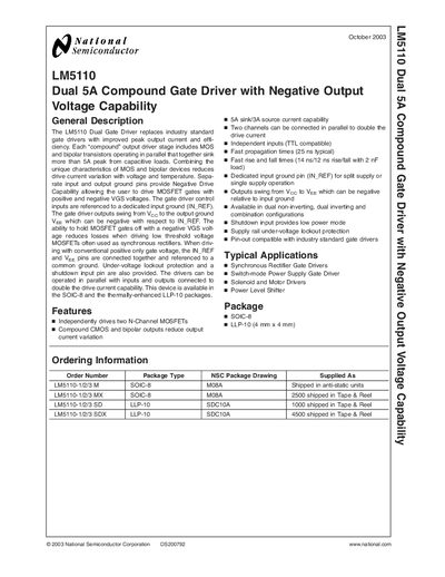
The LM5110 dual gate driver combines MOS and bipolar transistors to deliver over 5 A peak sink current and 3 A source current, with independent inputs and split‑ground pins that enable negative VGS drive. It supports both single‑supply and split‑supply configurations, allowing MOSFET gates to be driven positive or negative for reduced loss in synchronous rectifier applications.
The device is offered in SOIC‑8 and thermally‑enhanced LLP‑10 packages, includes under‑voltage lockout, shutdown control, and can be paralleled for doubled drive capability. Detailed electrical characteristics, pin descriptions, and mechanical dimensions are provided for design integration.
| Sink Current | 5 A |
|---|---|
| Source Current | 3 A |
| Propagation Delay (typical) | 25 ns |
| Rise Time (2 nF load) | 14 ns |
The LM5110 can sink up to 5 A of current.
Typical propagation delay is about 25 ns.
Yes, the separate input and output grounds provide negative drive capability for VGS.
The device is offered in SOIC‑8 and thermally‑enhanced LLP‑10 packages.