
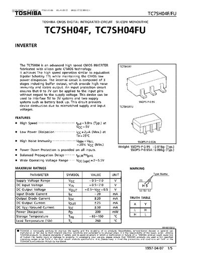
The TC7SH04F/FU is a CMOS digital integrated circuit inverter fabricated with silicon‑gate C2MOS technology. It offers high‑speed operation comparable to bipolar Schottky TTL while maintaining the low power consumption of CMOS, and includes input protection for 0‑7 V signals.
Key specifications include a supply voltage range of 2.0 V–5.5 V, power‑down protection on all inputs, and a typical package weight of 0.016 g (SSOP5‑P‑0.95) or 0.006 g (SSOP5‑P‑0.65). The device is rated for 200 mW power dissipation and can operate from –40 °C to 85 °C.
| Supply Voltage (Vcc) | 2.0 V – 5.5 V |
|---|---|
| Input Voltage (VIN) | 0 V – 5.5 V |
| Output Voltage (VOUT) | 0 V – Vcc+0.5 V |
| Power Dissipation (PD) | 200 mW |
| Storage Temperature | -65 °C – 150 °C |
| Lead Temperature (10 s) | 260 °C |
| Input Diode Current | -20 mA |
| Output Diode Current | +20 mA |
| DC Output Current | 425 mA |
| Package Weight (SSOP5‑P‑0.95) | 0.016 g (typ.) |
| Package Weight (SSOP5‑P‑0.65) | 0.006 g (typ.) |
The device operates with a supply voltage (Vcc) from 2.0 V to 5.5 V.
It is offered in SSOP5‑P‑0.95 (≈0.016 g) and SSOP5‑P‑0.65 (≈0.006 g) packages.
The maximum power dissipation is 200 mW.
The device is specified for –40 °C to 85 °C ambient temperature.