
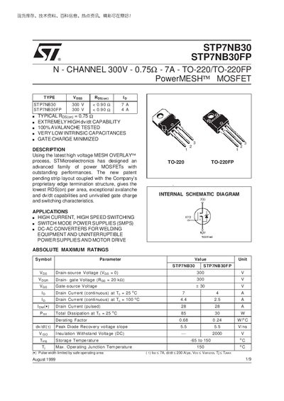
The STP7NB30 and STP7NB30FP are high‑voltage N‑channel power MOSFETs built on STMicroelectronics' MESH™ overlay process. They feature very low on‑resistance, high avalanche capability, fast switching and minimized gate charge, making them suitable for demanding power conversion applications.
Typical applications include high‑current, high‑speed switching, switch‑mode power supplies, DC‑AC converters for welding equipment, uninterruptible power supplies and motor drives. The document lists absolute maximum ratings, thermal data, detailed electrical characteristics, switching parameters and mechanical dimensions for both the TO‑220 and TO‑220FP packages.
| Drain‑source voltage (VDS) | 300 V |
|---|---|
| Gate‑source voltage (VGS) | +30 V |
| Continuous drain current (ID) at 25 °C | 7 A (STP7NB30) / 4 A (STP7NB30FP) |
| Continuous drain current (ID) at 100 °C | 4.4 A (STP7NB30) / 2.5 A (STP7NB30FP) |
| On‑resistance (RDS(on)) typical | 0.75 Ω (STP7NB30) / 0.90 Ω (STP7NB30FP) |
| Maximum power dissipation (PD) | 85 W (STP7NB30) / 30 W (STP7NB30FP) |
| Avalanche current (IAval) | 7 A |
| Total gate charge (Qg) | 17 nC |
Both devices are rated for a maximum drain‑source voltage of 300 V.
The typical on‑resistance is 0.75 Ω for the STP7NB30 and 0.90 Ω for the STP7NB30FP.
The STP7NB30 can handle 7 A continuously, while the STP7NB30FP is rated for 4 A at 25 °C.
The TO‑220 version (STP7NB30) can dissipate up to 85 W, and the TO‑220FP version (STP7NB30FP) up to 30 W.