
STMicroelectronics announces the STB7N52K3 to STP7N52K3 series N-channel 525 V, 0.84Ω, 6.3 A SuperMESH3™ Power MOSFETs. These devices integrate ST's established PowerMESH™ layout with a further fine tuning and new optimization of the vertical structure, combining a significant on-resistance reduction over previous generation with special attention to ensure a very good dv/dt capability and higher margin in breakdown voltage for the most demanding application.
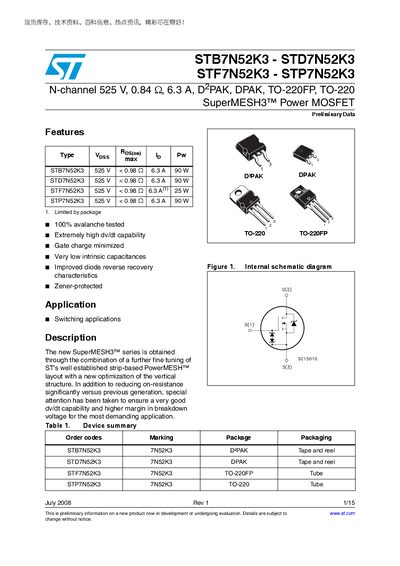
This datasheet provides the electrical ratings, characteristic curves and mechanical data for the STB7N52K3, STD7N52K3, STF7N52K3 and STP7N52K3 SuperMESH3™ Power MOSFETs. It includes absolute maximum ratings, on/off state parameters, switching times and avalanche specifications.
The document also lists the available package types (DPAK, D?PAK, TO‑220, TO‑220FP), mechanical dimensions, test circuit examples and revision history. All information is preliminary and subject to change without notice.
| Drain‑source voltage (VDS) | 525 V |
|---|---|
| Gate‑source voltage (VGS) | 30 V |
| Maximum junction temperature (Tj) | 150 °C |
| Package types | DPAK, D?PAK, TO‑220, TO‑220FP |
The MOSFETs are rated for a maximum drain‑source voltage of 525 V.
They are offered in DPAK, D?PAK, TO‑220 and TO‑220FP packages.