
This datasheet presents the characteristics of the STB75NF75, STP75NF75 and STP75NF75FP N-channel power MOSFET series manufactured with STMicroelectronics unique STripFET™ process. This series is designed to minimize input capacitance and gate charge, making it suitable for use as primary switch in advanced high-efficiency, high-frequency isolated DC-DC converters for Telecom and Computer applications. It is also intended for any applications with low gate drive requirements.
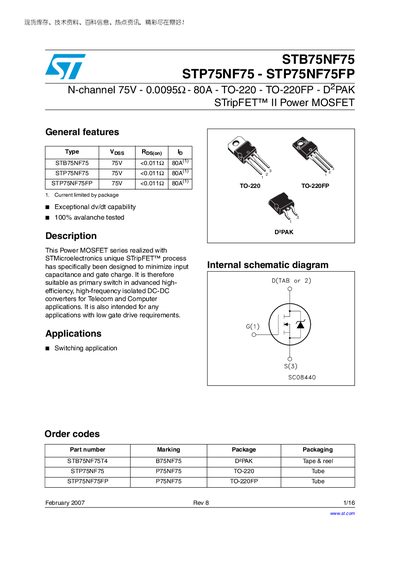
The STB75NF75, STP75NF75 and STP75NF75FP are N‑channel 75 V Power MOSFETs realized with STMicroelectronics' STripFET™ process. They are designed for low input capacitance and gate charge, making them suitable as primary switches in high‑efficiency, high‑frequency isolated DC‑DC converters for telecom and computer applications, as well as other low‑gate‑drive requirements.
Key specifications include a maximum drain‑source voltage of 75 V, continuous drain current of 80 A at 25 °C, pulsed drain current of 320 A, and total power dissipation up to 300 W (DPAK) or 45 W (TO‑220FP). The devices operate over a temperature range of –55 °C to 175 °C and feature thermal resistance values as low as 0.5 °C/W (junction‑case).
| Drain‑source voltage (Vds) | 75 V |
|---|---|
| Pulsed drain current | 320 A |
| Thermal resistance junction‑case (Rjc) | 0.5 °C/W |
| Thermal resistance junction‑ambient (Rja) | 62.5 °C/W |
| Operating temperature range | -55 °C to 175 °C |
The maximum drain‑source voltage is 75 V.
They operate from –55 °C to 175 °C.