
The PX3511A and PX3511B are high frequency MOSFET drivers specifically designed to drive upper and lower power N-Channel MOSFETs in a synchronous rectified buck converter topology. These drivers combined with the ISL6595 Digital Multi-Phase Buck PWM controller and N-Channel MOSFETs form a complete core-voltage regulator solution for advanced microprocessors. The PX3511A drives the upper gate to 12V, while the lower gate can be independently driven over a range from 5V to 12V. The PX3511B drives both upper and lower gates over a range of 5V to 12V. This drive-voltage provides the flexibility necessary to optimize applications involving trade-offs between gate charge and conduction losses. An adaptive zero shoot-through protection is integrated to prevent both the upper and lower MOSFETs from conducting simultaneously and to minimize the dead time. These products add an overvoltage protection feature operational before VCC exceeds its turn-on threshold, at which the PHASE node is connected to the gate of the low side MOSFET (LGATE). The output voltage of the converter is then limited by the threshold of the low side MOSFET, which provides some protection to the microprocessor if the upper MOSFET(s) is shorted during initial start-up.
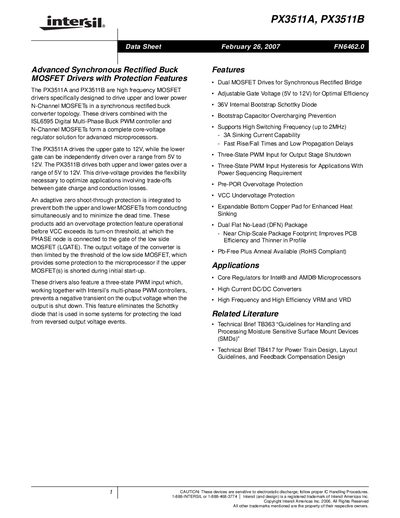
The PX3511A and PX3511B are synchronous rectified buck MOSFET drivers designed for upper and lower N‑Channel power MOSFETs. PX3511A provides a fixed 12 V upper‑gate drive and a 5 V‑12 V adjustable lower‑gate drive, while PX3511B drives both gates from a common 5 V‑12 V rail. Integrated adaptive zero‑shoot‑through, pre‑POR over‑voltage protection, and a three‑state PWM shutdown window help prevent shoot‑through and negative transients.
These devices support switching frequencies up to 2 MHz, offer 3 A sinking current capability, and are available in a 3 × 3 mm DFN package with an exposed thermal pad. Recommended operating conditions include a 0 °C‑85 °C ambient range and a maximum junction temperature of +150 °C.
| Adjustable Gate Voltage | 5 V to 12 V |
|---|---|
| Maximum Switching Frequency | 2 MHz |
| Sinking Current Capability | 3 A |
| Ambient Temperature Range | 0 °C to +85 °C |
| Maximum Junction Temperature | +150 °C |
| Package Power Dissipation (SO8) | ≈800 mW at room temperature |
The PX3511A drives the upper gate to 12 V, while the lower gate can be independently driven over a range from 5 V to 12 V.
They include adaptive zero shoot‑through protection, pre‑POR over‑voltage protection, and a three‑state PWM input shutdown window that disables the outputs when the PWM signal stays within the window.
The devices support switching frequencies up to 2 MHz.