
This document is the ADG752 product manual, which introduces its main features and characteristics.
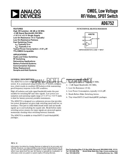
The ADG752 is a CMOS low‑voltage SPDT switch designed for audio, video, RF, networking, battery‑powered and communication applications. Its T‑switch configuration provides excellent off isolation while maintaining good on‑state frequency response, making it suitable for high‑frequency signal routing and relay replacement.
The device operates from a single supply of +1.8 V to +5.5 V, features a typical on‑resistance of 15 Ω, off isolation of –80 dB at 30 MHz, and a –3 dB bandwidth of 250 MHz. It is available in 6‑lead SOT‑23 (RT‑6) and 8‑lead HSOIC (RM‑8) packages, with recommended PCB layout and decoupling practices to preserve performance at high frequencies.
| Off Isolation | -80 dB at 30 MHz |
|---|---|
| Signal Bandwidth (‑3 dB) | 250 MHz |
| Typical On‑Resistance | 15 Ω |
| Power Consumption | < 0.01 pW |
| Switching Time (t_on) | 8 ns typical |
| Supply Voltage Range | +1.8 V to +5.5 V |
The typical on‑resistance is 15 Ω.
It operates from a single supply of +1.8 V to +5.5 V.
The device provides –80 dB off isolation at 30 MHz.