
This document describes the features and characteristics of the ADG417 LC2MOS precision mini-DIP analog switch, including maximum voltage supply, low on resistance, ultra-low power dissipation, and fast switching times. The product is suitable for precision test equipment, precision instrumentation, battery powered systems, and sample hold systems.
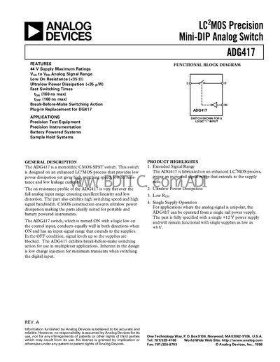
The ADG417 analog switch is built on an enhanced LC‑MOS process, delivering low on‑resistance (<35 Ω), ultralow power dissipation and fast switching. It operates from dual or single supplies and is suited for precision test equipment, battery‑powered instruments and sample‑hold applications.
The datasheet provides detailed specifications, absolute maximum ratings, typical performance curves, package dimensions and ordering information for the N‑8 DIP and S‑8 SOIC versions.
| Supply Voltage Range (Dual) | +4 V to +15 V (±10 %) |
|---|---|
| On‑Resistance (Ron) typical | <35 Ω |
| Input High Voltage (Vih) | 24 V min |
| Input Low Voltage (Vil) | 0.8 V max |
| Switch‑on delay (ton) | 160 ns max |
| Switch‑off delay (torr) | 100 ns max |
The device supports an analog signal range from Vss to Vpp.
The part can dissipate up to 400 mW.