
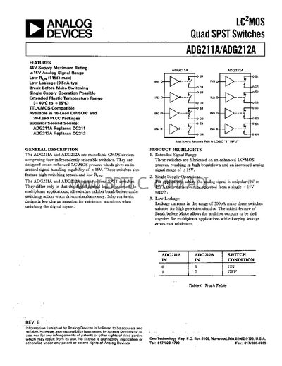
The ADG211A and ADG212A are monolithic CMOS quad SPST switches designed for analog signal routing. They operate from a single +15 V supply, provide break‑before‑make switching, and feature low charge injection for precision applications.
Key specifications include a 44 V maximum supply rating, ±15 V analog signal range, typical on‑resistance of 115 Ω, off‑leakage of 0.5 nA, and propagation delays as low as 30 ns. The devices are offered in N‑16 (DIP), R‑16A (SOIC) and P‑20A (PLCC) packages, with ordering codes ADG211AKN, ADG211AKR, ADG211AKP, ADG212AKN, ADG212AKR, ADG212AKP.
| Maximum Supply Voltage | 44 V |
|---|---|
| Analog Signal Range | ±15 V |
| On‑Resistance (Ron) typical | 115 Ω |
| Off‑Leakage Current (I_OFF) | 0.5 nA typ |
| Propagation Delay (t_on) | 30 ns typ |
The devices are rated for a maximum supply voltage of 44 V.
They support an analog signal range of ±15 V.
Typical on‑resistance is 115 Ω.
Off‑state leakage current is typically 0.5 nA.