
AD5371 is a 40-channel, 14-bit, serial input, voltage output DAC with system calibration function, user-programmable offset and gain, channel grouping and addressing features, thermal shutdown function, DSP/microcontroller-compatible serial interface, SPI/LVDS serial interface, 2.5 V to 5.5 V digital interface, digital reset (RESET), clear function to user-defined SIGGNDx, simultaneous update of DAC outputs
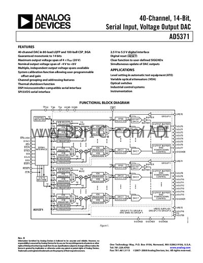
The AD5371 is a 40‑channel, 14‑bit digital‑to‑analog converter offered in 80‑lead LQFP and 100‑ball CSP‑BGA packages. It features buffered voltage outputs with programmable gain and offset, multiple independent output spans, and a high‑speed serial interface compatible with SPI, LVDS, and DSP standards.
The document includes a functional block diagram, detailed specifications, timing characteristics, power‑supply recommendations, and example interfacing circuits for DSPs and microcontrollers. It also covers calibration, power‑down, thermal shutdown, and layout guidelines to ensure accurate performance.
| Resolution | 14 Bits |
|---|---|
| Integral Nonlinearity (INL) | -1 to +1 LSB |
| Differential Nonlinearity (DNL) | -1 to +1 LSB |
| Gain Error | 0.1 % FSR |
| Nominal Output Voltage Range | -4 V to +8 V |
| Digital Supply Voltage (DVcc) | 2.5 V to 5.5 V |
The device can handle clock speeds of up to 50 MHz.
The AD5371 contains 40 independent 14‑bit DAC channels.
The nominal output voltage span is –4 V to +8 V (maximum 4 × Vref, up to 20 V).
It requires DVcc 2.5 V–5.5 V, Vop 9 V–16.5 V, and Vss –16.5 V to –8 V.