
This document is the datasheet of Analog Devices' product ADF4350, which mainly introduces the output frequency range, frequency synthesis mode, output power and other characteristics of the product
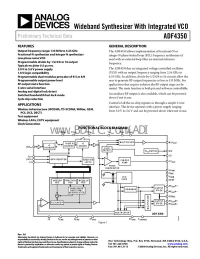
The ADF4350 is a wideband frequency synthesizer with an integrated VCO, offering output frequencies from 135 MHz to 4.35 GHz and supporting both fractional‑N and integer‑N PLL operation. It operates from a 3.0 V–3.6 V supply and includes features such as programmable divide‑by‑1/2/4/8/16, RF mute, and a 3‑wire serial interface.
This handbook compiles the device’s specifications, pin descriptions, timing diagrams, absolute maximum ratings, and programming details, along with application notes for wireless infrastructure, test equipment, and clock generation. It also provides design guidelines, ordering information, and example configurations.
| Output frequency range | 135 MHz to 4.35 GHz |
|---|---|
| Power supply voltage | 3.0 V to 3.6 V |
| Reference input frequency | 10 MHz to 250 MHz |
| VCO output frequency range | 2.16 GHz to 4.35 GHz |
| Operating temperature range | –40 °C to +85 °C |
| Output power | –6 dBm to +3 dBm |
| Phase noise (2.2 GHz carrier, 10 kHz offset) | –89 dBc/Hz |
| Package | 32‑Lead Lead Frame Chip Scale Package (LFCSP) |
The device can generate RF output frequencies from 135 MHz up to 4.35 GHz.
It operates from a supply voltage between 3.0 V and 3.6 V.
Pulling the PDBrr pin low mutes the RF outputs; the mute function can also be controlled by software.
The reference input can accept frequencies from 10 MHz to 250 MHz.