
This document describes the features and characteristics of the AD8012* dual 350 MHz low power amplifier. The amplifier is characterized by low power consumption, high output current, high speed, and low distortion, making it suitable for various applications.
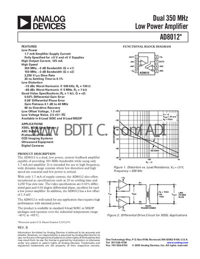
The AD8012 is a dual, low‑power current‑feedback amplifier designed for high‑frequency, wide‑dynamic‑range systems where low distortion and high speed are essential. It is suited for XDSL, HD‑S, CCD imaging, ultrasound equipment, and digital cameras, operating over an industrial temperature range of –40 °C to +85 °C.
The device provides up to 350 MHz –3 dB bandwidth, 2,250 V/µs slew rate, 20 ns settling time, 125 mA output current, and low offset voltage (1.5 mV). It is available in 8‑lead SOIC and 8‑lead MSOP packages, with absolute maximum ratings of 0.8 W (SOIC) and 0.6 W (MSOP).
| Supply Current per Amplifier | 1.7 mA |
|---|---|
| Small‑Signal Bandwidth (G=+1) | 350 MHz |
| Slew Rate | 2,250 V/µs |
| Settling Time (0.1 % to 2 Vpp) | 20 ns |
| Output Current (max) | 125 mA |
| Operating Temperature Range | -40 °C to +85 °C |
| Absolute Maximum Power Dissipation (SOIC) | 0.8 W |
| Absolute Maximum Power Dissipation (MSOP) | 0.6 W |
Each amplifier draws 1.7 mA of supply current.
The device can source up to 125 mA of output current.
It operates from –40 °C to +85 °C.
The SOIC package can dissipate up to 0.8 W.