
ADA4960-1 is a 5 GHz low distortion ADC driver/line driver. It features programmable gain, differential or single-ended input, differential output, low harmonic distortion, etc.
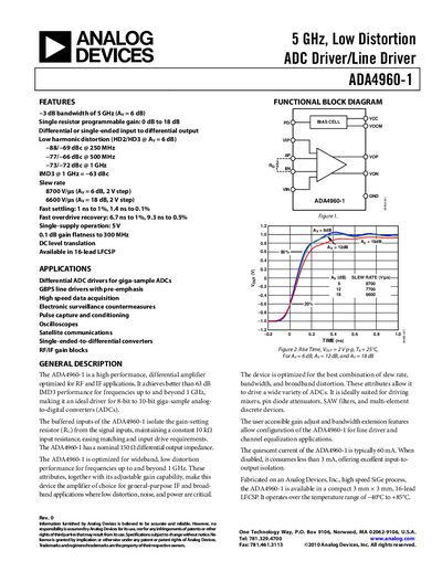
The ADA4960-1 differential amplifier from Analog Devices is optimized for RF and IF use, offering a programmable gain of 0‑18 dB, single‑supply operation at 5 V, and a nominal 150 Ω differential output impedance. It features a very high slew rate, fast settling, and low harmonic distortion, making it suitable for driving high‑speed ADCs, mixers, and other broadband circuits.
The datasheet provides detailed specifications, absolute maximum ratings, pin descriptions, typical performance graphs, layout recommendations, and ordering information. It also includes over‑drive recovery data and thermal management guidance for high‑speed PCB designs.
| Bandwidth (‑3 dB) | 5 GHz (AV = 6 dB) |
|---|---|
| Slew Rate | 8700 V/µs (AV = 6 dB) |
| Quiescent Current (ENB high) | Typical 60 mA |
| Supply Voltage | 5 V (absolute max 5.25 V) |
| Differential Output Impedance | 150 Ω |
| Input Resistance (Differential) | 10 kΩ |
| Operating Temperature Range | ‑40 °C to +85 °C |
The device draws about 60 mA in its normal enabled state and less than 3 mA when disabled.
The absolute maximum supply voltage is 5.25 V.
Recovery is 6.7 ns to 1 % and 9.3 ns to 0.5 % of the final output voltage.