
XP162A12A6PR-G is a P-channel Power MOSFET from Infineon with low on-state resistance and ultra high-speed switching characteristics. Because high-speed switching is possible, the IC can be efficiently set thereby saving energy. A gate protect diode is built-in to prevent static damage. The small SOT-89 package makes high density mounting possible.
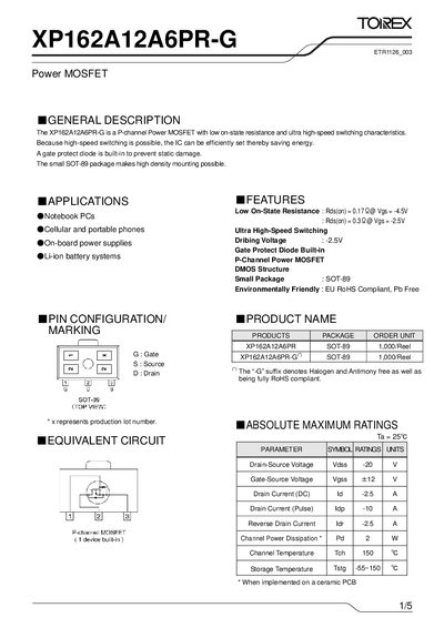
The XP162A12A6PR-G is a P‑channel Power MOSFET designed for low on‑state resistance (Rds(on) = 0.172 Ω at Vgs = -4.5 V) and ultra‑high‑speed switching. It includes a built‑in gate protect diode and is supplied in a compact SOT‑89 package, making it suitable for high‑density mounting in notebook PCs, cellular phones, on‑board power supplies and Li‑ion battery systems. The device is RoHS compliant, halogen‑ and antimony‑free.
The datasheet lists absolute maximum ratings such as Vdss = -20 V, Vgss = +12 V, Id (DC) = -2.5 A, Idp (pulse) = -10 A, and a channel power dissipation of 2 W. Detailed electrical characteristics are provided, including DC and dynamic parameters, switching times, capacitances, and thermal resistance (Rth(ch‑a) = 62.5 °C/W on a ceramic PCB). Typical performance curves illustrate the relationship between drain current, on‑state resistance, and temperature.
| On‑State Resistance (Rds(on)) @ Vgs = -4.5 V | 0.172 Ω |
|---|---|
| On‑State Resistance (Rds(on)) @ Vgs = -2.5 V | 0.32 Ω |
| Drain‑Source Voltage (Vdss) | -20 V |
| Gate‑Source Voltage (Vgss) | +12 V |
| Continuous Drain Current (Id) at 25 °C | -2.5 A |
| Pulse Drain Current (Idp) | -10 A |
| Channel Power Dissipation (Pd) | 2 W |
| Storage Temperature Range | -55 °C to 150 °C |
The on‑state resistance is 0.172 Ω at Vgs = -4.5 V.
It is supplied in a small SOT‑89 package.
Yes, the device is fully RoHS compliant and free of halogen and antimony.
The maximum drain‑source voltage is -20 V and the maximum gate‑source voltage is +12 V.