
TC74VHC00F, TC74VHC00FT, and TC74VHC00FK are quad 2-input NAND gate products released by Toshiba. They use CMOS technology and have the characteristics of low power consumption and high-speed operation comparable to Schottky TTL. The newly adopted Q&Q buffer greatly reduces various noises generated during switching. The internal circuit is a 3-stage configuration with buffers, providing high noise margin and stable output. All input terminals adopt a newly developed input protection circuit that does not include a diode on the positive side (toward VCC from the input), allowing input voltages of 5.5V to be applied even without the power supply voltage. This input power-down protection method enables a wide range of applications, including 2 power supply interface, level conversion from 5V to 3V system, and battery backup circuits.
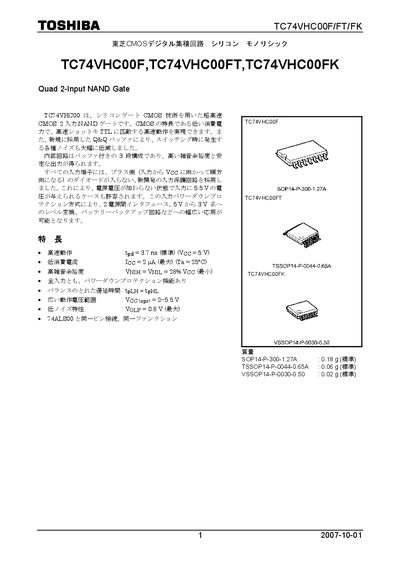
The TC74VHC00F/FT/FK is a CMOS quad 2‑input NAND gate offering high‑speed operation and low power consumption. It features input protection that allows up to 5.5 V on inputs without a supply voltage, making it suitable for level‑shifting and battery‑backup applications.
Key specifications include a typical propagation delay of 3.7 ns, a maximum supply current of 2 nA, a wide operating voltage range of 2.0‑5.5 V, and an operating temperature range of –40 °C to 85 °C. Package options are SOP14, TSSOP14, and VSSOP34 with masses as low as 0.02 g. This manual is written in Japanese.
| Propagation delay (tpd) | 3.7 ns (typical) |
|---|---|
| Supply current (ICO) | 2 nA (max) |
| Operating temperature range | -40 °C to 85 °C |
| Package mass (SOP14) | 0.18 g (standard) |
The typical propagation delay is 3.7 ns.
The maximum supply current is 2 nA.
The device is rated for –40 °C to 85 °C.