
The TC74VCX162721FT is a high-performance CMOS 20-bit D-type flip-flop. Designed for use in 1.8V, 2.5V or 3.3V systems, it achieves high-speed operation while maintaining the CMOS low power dissipation. It is also designed with overvoltage tolerant inputs and outputs up to 3.6V. The TC74VCX162721FT is an edge-triggered D-type flip-flop with qualified clock storage. On the positive transition of the clock (CK) input, the device provides true data at the Q outputs if the clock-enable (CKEN) input is low. If CKEN is high, no data is stored. When the OE input is high, the outputs are in a high-impedance state. This device is designed to be used with 3-state memory address drivers, etc. The 26-Ω series resistor helps reducing output overshoot and undershoot without external resistor. All inputs are equipped with protection circuits against static discharge.
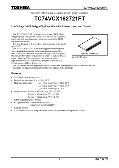
The TC74VCX162721FT is a high‑performance CMOS 20‑bit D‑type flip‑flop with low‑voltage operation (1.8‑3.6 V) and 3.6‑V tolerant inputs and outputs. It features edge‑triggered clock storage, clock‑enable control, and three‑state outputs suitable for memory address drivers.
The document provides detailed electrical characteristics, absolute maximum ratings, timing parameters, package dimensions, and usage restrictions for general electronics applications.
| Package | TSSOP |
|---|---|
| Supply voltage range (Voc) | 0.5 V to 4.6 V |
| Operating temperature | ‑40 °C to 85 °C |
| Propagation delay (tpLH) | 4.4 ns (max) |
| Output current (Ion/loL) | +12 mA (min) |
The device is supplied in a TSSOP package.
It operates with a supply voltage from 0.5 V up to 4.6 V.
The device can operate from –40 °C to 85 °C.
The maximum propagation delay is 4.4 ns.