
TC74AC112P/F/FN is an advanced high speed CMOS DUAL J-K FLIP FLOP fabricated with silicon gate and double-layer metal wiring C2MOS technology. It achieves the high speed operation similar to equivalent Bipolar Schottky TTL while maintaining the CMOS low power dissipation.
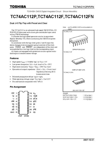
The TC74AC112 is an advanced high‑speed CMOS dual J‑K flip‑flop with preset and clear, fabricated using silicon gate and double‑layer metal C2MOS technology. It offers high speed comparable to bipolar Schottky TTL while maintaining low CMOS power dissipation, with features such as 170 MHz typical fmax, 4 µA supply current, and 28 % Vcc noise immunity.
The device operates over a 2.0 V to 5.5 V supply range, supports temperatures from –40 °C to 85 °C, and is available in DIP16, SOP16, and SOL16 packages. Detailed electrical characteristics, timing requirements, and package dimensions are provided, along with usage restrictions and reliability guidelines for designers.
| Maximum operating frequency (fmax) | 170 MHz (typ.) |
|---|---|
| Noise immunity (VNIH/VNIL) | 28 % Vcc (min) |
| Symmetrical output impedance | 24 mA (min) |
| Power dissipation | 500 mW (DIP) / 180 mW (SOP) |
| Storage temperature | -65 °C to 150 °C |
| DIP16 package dimensions | 16 mm × 9 mm |
| DIP16 package weight | 1.00 g (typ.) |
| SOP16 package dimensions | 16 mm × 9 mm |
| SOP16 package weight | 0.18 g (typ.) |
The device achieves a typical maximum frequency of 170 MHz at a 5 V supply.