
The NE650R279A is a 0.2W GaAs MES FET designed for middle power transmitter applications for mobile communication handset and base station systems. It is capable of delivering 0.2 watt of output power (CW) with high linear gain, high efficiency, excellent distortion and is suitable as a driver amplifier for our NE6500379A etc.
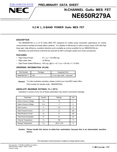
The NE650R279A is a 0.2 W N-channel GaAs MES FET for middle-power transmitter applications in mobile communication handset and base station systems. The preliminary data sheet states that it can deliver 0.2 watt CW output power and is suitable as a driver amplifier for devices such as the NE6500379A.
The document gives absolute maximum ratings, recommended operating limits, electrical characteristics, S-parameters from 1400 to 3000 MHz, an application circuit example, 79A package dimensions, a recommended PC board layout, and soldering conditions.
| Output Power at 1 dB Gain Compression | +23 dBm typ. |
|---|---|
| Linear Gain | 16 dB typ. |
| Power Added Efficiency | 45% typ. |
| Drain to Source Voltage (max) | 15 V |
| Total Power Dissipation | 2.1 W |
| Channel Temperature (max) | 150 °C |
| Saturated Drain Current | 150 mA |
| Thermal Resistance, channel to case | 40 to 60 °C/W |
| Package | 79A |
It is a 0.2 W GaAs MES FET designed for middle-power transmitter applications in mobile communication handset and base station systems.
It is capable of delivering 0.2 watt of output power (CW).
The recommended drain to source voltage is 6.0 V.
The package peak temperature should be 235°C or below, with 30 seconds or less at 210°C and a count of 2.