
ST STP25NM50N STF25NM50N STB25NM50N/-1 STW25NM50N handbook

The STx25NM50N is realized with the second generation of MDmesh Technology. This revolutionary MOSFET associates a new vertical structure to the Company's strip layout to yield one of the world's lowest on-resistance and gate charge. It is therefore suitable for the most demanding high efficiency converters
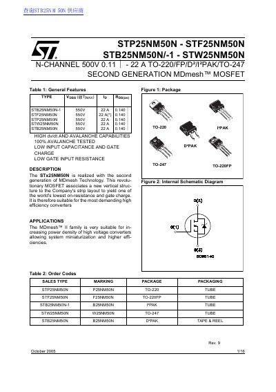

ST STP25NM50N STF25NM50N STB25NM50N/-1 STW25NM50N handbook - cover page
Brand
STMicroelectronics
Category
MOSFET
Document type
Datasheet
Language
English
Pages
16
File format
PDF
File size
421 KB
Published
07 August, 2012
Updated
30 September, 2023
Model
STB1
MD5 checksum
F3459DDA65E3388274EA313A42D54E44

About this manual

This document describes the STx25NM50N family of N-channel MOSFETs, which utilize the second generation of MDmesh Technology. These devices are designed to offer one of the world's lowest on-resistance and gate charge, making them suitable for high-efficiency converters and demanding high-voltage applications.

What's inside

  • General Features
  • Absolute Maximum Ratings
  • Thermal Data
  • Electrical Characteristics
  • Safe Operating Area
  • Package Information
  • Revision History

Specifications

Storage Temperature-55 to 150 °C

Frequently asked questions

What is the maximum continuous drain current for this MOSFET at a case temperature of 25°C?

The device supports a continuous drain current of 22 A when the case temperature is 25°C.

What are the maximum ratings for drain-source and gate-source voltage?

The maximum drain-source voltage is 500 V, and the maximum gate-source voltage is 425 V.

What is the typical static drain-source on-resistance when the gate-source voltage is 10 V?

The typical static drain-source on-resistance is 0.140 Ω at a gate-source voltage of 10 V.

Download PDF (421 KB)

More STMicroelectronics Manuals


View all STMicroelectronics manuals →