
This Engineering Note demonstrates how to interface a 5v FLASH memory to an ADSP- 218x DSP. The supplied code shows you how to program, erase, and retrieve device ID
This Engineering Note (EE-39) describes how to interface 5V Flash memories to the ADSP-218x Digital Signal Processor. It details the wiring connections between the DSP and Flash devices via the BDMA port and explains the byte-by-byte programming protocol used by AMD Flash memories. The document covers operations such as autoselect, byte write, sector erase, and chip erase.
| Interface Port | BDMA |
|---|---|
| Programming Protocol | byte-by-byte |
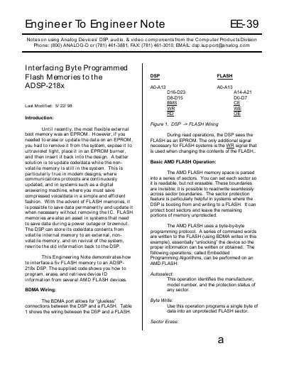
The WR signal is the only additional signal necessary for Flash systems when changing the contents of the Flash.
It can be countered with a simple RC network attached to each data pin and to ground (R=120 Ω, C=47pF).
A sector or chip erase operation is the only operation that converts a logic '0' to a logic '1'.