
The document is a technical note on using Analog Devices' DSP components and development tools. It provides information on correctly setting mode pins in a design and offers general guidelines.
This document is an Engineer-to-Engineer Note (EE-64) from Analog Devices regarding the use of DSP components and development tools. It addresses specific design questions concerning the ADSP-218x series of Digital Signal Processors (DSPs).
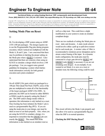
The note provides guidance on handling multiplexed Mode pins (Mode A, B, and C) which are used for booting in BDMA or IDMA modes. It explains that these settings are latched only on reset and offers two methods for setting them correctly: using static pull-up or pull-down resistors (recommended 10kΩ) or dynamic connections driven by RESET and ERESET signals. Additionally, it covers the requirements for supplying a CLKIN signal during the initial reset assertion to ensure stable internal register states before normal operation.
| Recommended Resistor Value | 10kΩ |
|---|---|
| Minimum Clock Cycles for Stable State | approximately twelve cycles |
| Minimum Clock Cycles Before Exiting Reset | at least 2000 cycles |
Care must be taken at reset to set them properly using either static pull-up/pull-down resistors or dynamic connections driven by RESET.
A resistor value of 10kΩ is recommended to minimize power dissipation and ensure correct biasing.
Yes, the ERESET pin acts exactly like RESET, meaning mode information is latched on an emulator reset as well as a chip reset.
It is necessary when RESET is first asserted to set initial internal register values and prevent transistors from being forced into an unknown state.