
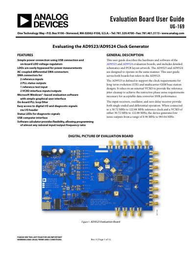
This document serves as the user guide for the AD9523 and AD9524 evaluation boards. It describes the hardware and software components, including detailed schematics and PCB layout artwork. The guide is applicable to both boards but primarily refers to the AD9523.
When connected to a 30.72 MHz to 122.88 MHz reference clock and a VCXO of either 30.72 MHz to 122.88 MHz, the device generates low noise outputs from a range of 0.96 MHz to 983.04 MHz.
An amplitude setting of 6 dBm is sufficient when connecting a signal generator to REF A SMA Connector J9.
To bypass the dc-to-dc converter only, you must connect a 2.2 V bench supply to Connector P19.