
This user guide describes the hardware of the AD9550 evaluation board. The AD9550 evaluation board is a compact, easy-to-use platform for evaluating all features of the AD9550 integer-N clock translator. The AD9550 is a phase-locked loop (PLL) based clock translator designed to address the needs of wireline communication and base station applications.
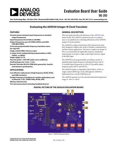
The document provides instructions for setting up power and signal connections on the AD9550 evaluation board. It details how to connect a 3.3 V CMOS reference input and measurement devices via SMA connectors.
The guide explains how to program the device using DIP switches (S1 through S4) to configure frequency translation ratios, output driver modes (LVPECL, LVDS, or CMOS), and PLL parameters based on specific pin combinations.
| Input Frequency Range | 8 kHz to 200 MHz |
|---|---|
| Output Frequency | up to 810 MHz |
| Supply Voltage | 3.3 V |
| Power Consumption | <450 mW |
| Operating Temperature | -40°C to +85°C |
The device supports LVPECL, LVDS, or single-ended CMOS logic levels for its two output clocks.
It is powered via the TB1 connector, where Pins 2-6 connect to a 3.3 V supply and Pins 1 and 5 connect to ground.
Settings are programmed via pin programming using DIP switches S1 through S4 to set logic levels on A, Y, and OM pins.