
The DS90CR286A and DS90CR216A are +3.3V rising edge data strobe LVDS receivers that convert LVDS data streams into parallel CMOS/TTL data streams. This chipset is an ideal solution for EMI and cable size problems associated with wide, high-speed TTL interfaces.
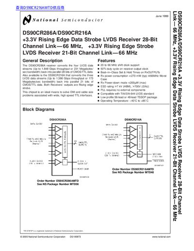
The document describes the DS90CR286A and DS90CR216A, which are +3.3V Rising Edge Data Strobe LVDS receivers. The DS90CR286A converts four LVDS data streams into parallel 28-bit CMOS/TTL data, while the DS90CR216A converts three streams into 21-bit data. Both operate at frequencies up to 66 MHz and are compatible with the TIA/EIA-644 LVDS standard.
| Shift Clock Support | 20 to 66 MHz |
|---|---|
| Supply Voltage | 3.0V to 3.6V |
| Operating Temperature | -40°C to +85°C |
| ESD Rating (HBM) | > 7 kV |
| Package Type | 56-lead or 48-lead TSSOP |
| Throughput (DS90CR286A) | Up to 1.848 Gbps |
| Throughput (DS90CR216A) | Up to 1.386 Gbps |
The receivers support a shift clock range from 20 to 66 MHz.
No, the PLL requires no external components.
The receiver power consumption is less than 200uW in power-down mode.