
DS90CR286A and DS90CR216A are +3.3V rising edge data strobe LVDS receivers that convert LVDS data streams into parallel CMOS/TTL data. This chipset is an ideal solution for solving EMI and cable size problems associated with wide, high-speed TTL interfaces.
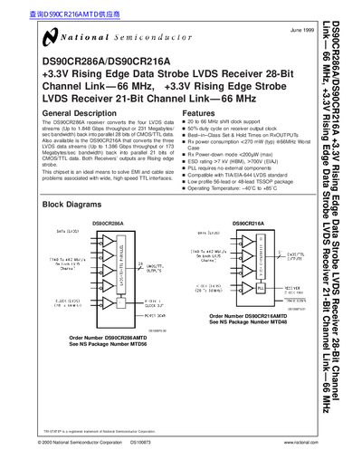
This document provides technical data for the DS90CR286A and DS90CR216A receivers from National Semiconductor. These chips convert four or three LVDS data streams back into parallel CMOS/TTL data with rising edge strobe outputs, operating at frequencies up to 66 MHz.
The datasheet details absolute maximum ratings, electrical characteristics including supply current and output voltage levels, receiver switching characteristics, and AC timing diagrams for setup/hold times and clock delays. It also includes physical dimensions for the available TSSOP packages.
| Supply Voltage (Vcc) | 3.0 V to 3.6 V |
|---|---|
| Operating Temperature Range | -40°C to +85°C |
| Max Shift Clock Frequency | 66 MHz |
| ESD Rating (HBM) | > 7 kV |
| Package Type | 56-lead or 48-lead TSSOP |
No, the internal PLL requires no external components.
The maximum supply voltage is 36 V for the DS90CR286A and 33 V for the DS90CR216A.
The maximum recommended operating temperature is +85°C.