
The LCX11 is a triple 3-input AND gate with buffered outputs. It is designed for low voltage (2.5V or 3.3V) operation with the added capability of interfacing to a 5V signal environment. The 74LCX11 is fabricated with advanced CMOS technology to achieve high speed operation while maintaining CMOS low power dissipation.
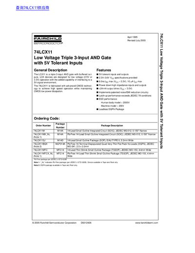
The 74LCX11 is a triple 3-input AND gate fabricated with advanced CMOS technology for high-speed operation at low voltages (2.5V or 3.3V). It features buffered outputs that are compatible with 5V signal environments, allowing interfacing between different voltage levels.
The device includes patented noise and EMI reduction circuitry and offers a power-down mode where inputs and outputs enter a high-impedance state. It is available in various packages including SOIC, SOP, TSSOP, and leadless DQFN.
| Propagation Delay (Max, Vcc=3.3V) | 6.0ns |
|---|---|
| Output Drive Current (Sourcing) | +24 mA |
| ESD Performance (Human Body Model) | > 2000V |
| Operating Temperature Range | -40°C to +85°C |
Yes, the device features 5V tolerant inputs and outputs.
The maximum propagation delay (tp) is 6.0ns when Vcc is 3.3V.