
The 74LCX112 is a low voltage (3.3V or 2.5) dual J-K negative edge-triggered flip-flop with 5V tolerant inputs that can interface to a 5V signal environment. The 74LCX112 is fabricated with advanced CMOS technology to achieve high speed operation while maintaining CMOS low power dissipation.
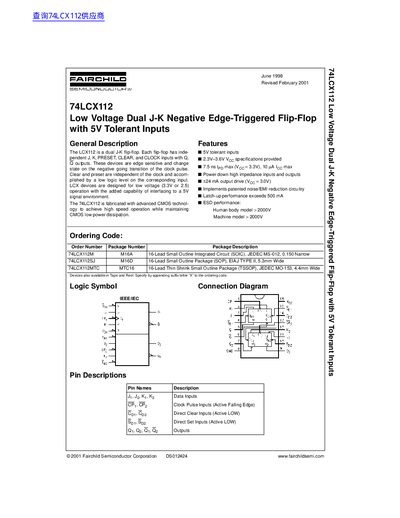
The 74LCX112 is a dual J-K flip-flop designed for low voltage operation (2.3V to 3.6V) with the capability to interface with 5V signal environments. Each flip-flop features independent J, K, PRESET, and CLEAR inputs, along with Q and Q outputs. The device is edge-sensitive, changing state on the negative going transition of the clock pulse, while clear and preset functions are independent of the clock and activated by a low logic level.
| Propagation Delay (Max) | 7.5 ns |
|---|---|
| Output Drive Current | +24 mA |
| Latch-up Performance | > 500 mA |
| ESD Performance (Human Body) | > 2000 V |
| Operating Temperature | -40 to 85 °C |
The flip-flops are edge sensitive and change state on the negative going transition of the clock pulse.
The maximum output drive current is +24 mA.