
The document describes the features and characteristics of the 74LCX11 low voltage triple 3-input AND gate, including 5V tolerant inputs, 2.3V-3.6V VCC specifications, and 6.0ns maximum delay.
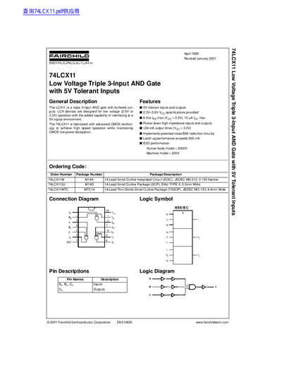
The document describes the 74LCX11, an integrated circuit fabricated with advanced CMOS technology. It is designed as a triple 3-input AND gate featuring buffered outputs, optimized for low voltage (2.5V or 3.3V) operation while maintaining compatibility with 5V signal environments.
| Propagation Delay (Max) | 6.0 ns |
|---|---|
| Output Drive Current (Max) | +24 mA |
| Latch-up Performance | > 500 mA |
| ESD Performance (Human Body) | > 2000V |
| Operating Temperature Range | -40 to +85 °C |
Yes, the device features 5V tolerant inputs and outputs.
The maximum propagation delay (tp) is 6.0 ns when Vcc is 3.3V.