
5476 is a dual master-slave J-K flip-flop with complementary outputs produced by National Semiconductor. It has two independent positive pulse triggers, which process J and K data after a complete clock pulse. When the clock is low, the slave is isolated from the master. When the clock is positive, the data from the J and K inputs is transferred to the master. When the clock is high, the J and K inputs are disabled. When the clock is negative, the data from the master is transferred to the slave. The logic state of J and K inputs must not be allowed to change while the clock is high. The data is transferred to the outputs on the falling edge of the clock pulse. When setting or resetting the outputs, a low logic level on the preset or clear inputs will be independent of the logic levels of the other inputs.
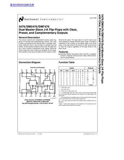
This document is a datasheet for the National Semiconductor 5476/DM5476/DM7476 series, which contains two independent positive pulse triggered J-K flip-flops with complementary outputs. The device features separate preset and clear inputs to set or reset the outputs regardless of other input levels. Data is transferred to the outputs on the falling edge of the clock pulse, provided the J and K inputs remain constant while the clock is high.
The datasheet provides absolute maximum ratings, recommended operating conditions, and electrical characteristics for both the DM54 series (military/aerospace) and DM74 series (commercial) variants. It includes a function table, switching characteristics, and physical dimensions for various package types, including Dual-In-Line, Molded Dual-In-Line, Ceramic Flat, and Ceramic Dual-In-Line packages.
| Supply Voltage | 4.5V to 5.5V (DM5476), 4.75V to 5.25V (DM7476) |
|---|---|
| Clock Frequency | 15 MHz |
| Operating Temperature Range (DM54) | -55°C to +125°C |
| High Level Output Voltage | 2.4V to 3.4V |
| Low Level Output Voltage | 0.2V to 0.4V |
The data is transferred to the outputs on the falling edge of the clock pulse.
No, the logic state of J and K inputs must not be allowed to change while the clock is high.
A low logic level on the preset or clear inputs will set or reset the outputs regardless of the logic levels of the other inputs.