
The MM74HC164 is an 8-bit serial-in/parallel-out shift register that utilizes advanced silicon-gate CMOS technology. It has the high noise immunity and low power consumption of standard CMOS integrated circuits, while offering speeds comparable to low power Schottky devices. This shift register has gated serial inputs and a CLEAR function. Each register bit is a D-type master/slave flip-flop. Inputs A and B provide complete control over the incoming data. A LOW level at either or both inputs inhibits the entry of new data and resets the first flip-flop to a low level at the next clock pulse. A high level on one input enables the other input to determine the state of the first flip-flop. Data at the serial inputs can be changed while the clock is HIGH or LOW, but only data that meets the setup and hold time requirements will be entered. Data is serially shifted in and out of the 8-bit register during the positive-going transition of the clock pulse. The CLEAR function is independent of the clock and is accomplished by a low level at the CLEAR input. The 74HC logic family is functionally and pin-out compatible with the standard 74LS logic family. All inputs are protected from damage due to static discharge by internal diode clamps to VCC and ground.
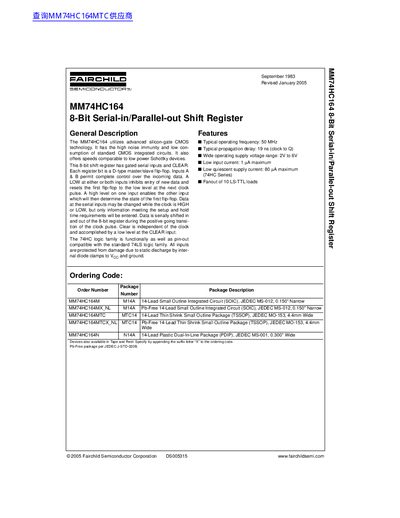
The MM74HC164 is an 8-bit serial-in/parallel-out shift register utilizing advanced silicon-gate CMOS technology. It features high noise immunity, low consumption, and speeds comparable to low power Schottky devices. The device includes gated serial inputs and a CLEAR function, with each register bit acting as a D-type master/slave flip-flop.
| Typical operating frequency | 50 MHz |
|---|---|
| Typical propagation delay | 19 ns (clock to Q) |
| Operating supply voltage range | 2V to 6V |
| Maximum input current | 1 uA |
| Maximum quiescent supply current | 80 pA |
| Fanout | 10 LS-TTL loads |
| Operating Temperature Range | -40 to +85 °C |
Clear is independent of the clock and is accomplished by a low level at the CLEAR input.
A LOW at either or both inputs A & B resets the first flip-flop to the low level at the next clock pulse.
Yes, the 74HC logic family is functionally as well as pin-out compatible with the standard 74LS logic family.