
The ABT16652 consists of sixteen bus transceiver circuits with D-type flip-flops, and control circuitry arranged for multiplexed transmission of data directly from the input bus or from the internal registers. Each byte has separate control inputs which can be shorted together for full 16-bit operation. Data on the A or B bus will be clocked into the registers as the appropriate clock pin goes to HIGH logic level. Output Enable pins (OEAB, OEBA) are provided to control the transceiver function.
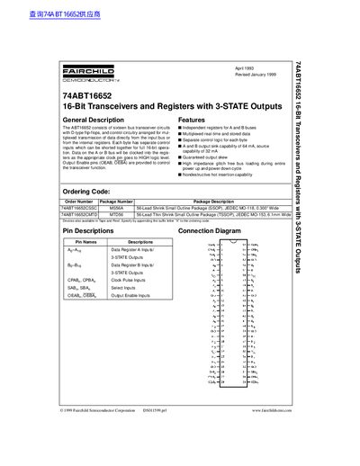
The document describes the ABT16652 device, which consists of sixteen bus transceiver circuits with D-type flip-flops. It supports multiplexed real-time and stored data transmission directly from input buses or internal registers, with separate control logic for each byte.
Key features include independent registers for A and B buses, guaranteed output skew, high impedance glitch-free bus loading during power cycles, and nondestructive hot insertion capability. The device is available in 56-lead SSOP and TSSOP packages.
| Output sink capability | 64 mA |
|---|---|
| Output source capability | 32 mA |
| Supply Voltage (Operating) | +4.5V to +5.5V |
| Free Air Ambient Temperature (Operating) | -40°C to +85°C |
| Max Clock Frequency | 200 MHz |
| Package Type (CSSC) | 56-Lead Shrink Small Outline Package |
The device has an A and B output sink capability of 64 mA.
Yes, it offers nondestructive hot insertion capability.